Articles
Self-Assembly Systems for Die Attachment: Magnet Assisted Alignment
Self-Assembly Systems for Die Attachment: Magnet Assisted Alignment

The method for self-aligning a first component and a second component using a patterned magnet. It further discloses modifying the magnetization of the patterned magnet to achieve the desired alignment accuracy. Furthermore, it discloses the types of magnets and structural features relevant to the self-alignment process between the first and second components. These components may include substrates, chips, wafers, dies, and similar elements.
Magnet Assisted Alignment Method for Wafer Bonding and Wafer Level Chip Scale Packaging
Summary of the Reference
Reference Provider:
YI GE (US); LIU ZONGRONG (US); TANG YUNJUN (US); LI SHAOPING (US)
Reference Proposed:
- The reference discloses alignment methodology for wafer-to-wafer or chip-to-wafer at high precision accuracy using the predetermined patterned magnet.
- Due to the specially designed magnet, external fields can activate or deactivate their pairing and modify their interaction force by adjusting the magnetization alignment.
Self-Alignment Technique Used:
- To align the first component and the second component, the reference uses patterned magnets to perform magnetization-based alignment.
Mechanism:
- Two components (i.e., wafers or chips) each comprising one or more patterned magnets.
- Bringing the two components to close proximity.
- By applying a magnetic field, the magnetizations of the patterned magnets in the two components become aligned.
- Subsequently, magnetic forces between the magnets tend to align them with each other, which in turn automatically aligns the two components.
Key Benefits:
- Improved alignment accuracy to sub-micron level.
- High unit-per-hour (UPH).
Application Areas:
Semiconductor Packaging and Fabrication
Related Resources:
- Self-Assembly Systems for Die Attachment: Overview
- Self-Assembly Systems for Die Attachment: Technology Study – Surface Tension of liquid
Summary of Semiconductor package structure and fabrication method thereof
Objective:
A method is provided for the self-alignment of a first component and a second component with sub-micron precision alignment accuracy, while achieving high units per hour (UPH) through a magnet-based alignment technique.
Reference Proposed:
The reference discloses specially designed patterned magnets integrated into the first and second components (wafer or chips). To perform self-alignment, the first and second components are brought into close proximity. The magnetic interlocking forces between the magnets in the two components facilitate self-alignment. Furthermore, the magnetization effect can be adjusted using an external magnetic field to enhance alignment accuracy.
Self-Alignment Technique Used:
- Magnet based Self alignment technology.
Mechanism:
- The first component and the second component are each integrated with patterned magnets.
- The two components are brought into close proximity.
- Magnetic forces between the patterned magnets facilitate self-alignment of the components.
- An external magnetic field is applied to influence the magnetization behavior.
- The external magnetic field is adjusted to enhance alignment accuracy in a sub-micron range.
Problem
A semiconductor package structure having:
- Low accuracy
- Less yield
- Low unit-per-hour (UPH)
Reference Proposed
An alignment methodology for wafer-to-wafer or chip-to-wafer integration using specially designed patterned magnets embedded in the first and second components.
When brought into close proximity, magnetic interlocking forces between the patterned magnets facilitate self-alignment with high precision.
The interaction between the magnets can be actively controlled by applying an external magnetic field, which adjusts the magnetization alignment.
This enables activation or deactivation of magnetic pairing and fine-tuning of the interaction force, thereby enhancing the overall alignment accuracy. Self-alignment with capability for sub-micron dynamic accuracy
Advantages
- Simultaneous high-precision alignment of multiple chips on a wafer is achieved through externally activated self-alignment using patterned magnets.
- External magnetic field control enables selective activation of the alignment process, improving accuracy and flexibility.
- High units per hour (UPH) is maintained due to parallel alignment and bonding of multiple chips.
Self-alignment Process & Key Aspects
Self-alignment Process Disclosed in this Patent
- By wafer-level processing, one or more patterned magnets and electrical connections are prepared on the first component near the bonding interface, along with corresponding mirror-shaped patterned magnets and electrical connections on the second component.
- Bringing the two components into close proximity to roughly align the magnet patterns, such that each magnet on the first component is approximately opposite its corresponding mirrored magnet on the second component.
- Applying a directionally controlled external magnetic field with preset strength variations to align the magnetizations, ensuring complementary pole alignment (north to south).
- Maintain the external magnetic field while bringing the components together, allowing magnetic forces to self-align the mirrored magnets for precise wafer-to-component alignment.
Key Aspect of the Invention
To achieve the alignment accuracy of sub micron range using magnet based self alignment. The wafer/ chips comprises patterned magnet and another wafer/chip comprises mirror shaped patterned magnet. Further, the patterned magnetic film can be soft magnetic film or the hard magnetic film.
Two different approaches to design our pairing patterned magnets:
Approach 1. Uses densely paired patterned magnets, implying that the magnets occupy not only the dicing area but also extend into portions of the device area. For this the patterned magnets must be designed such that the magnetic flux leakage between the paired magnets is minimized and approaches zero after bonding.
Approach 2. Primarily utilizes the dicing areas or edge regions, with patterned magnets designed to have large surface areas facing each other.
In the case where multiple patterned magnets are used on the first component (wafer or chip) and multiple mirror-shaped patterned magnets on the second component, the gap between adjacent magnets is intentionally made sufficiently large to prevent misalignment errors after coarse alignment, ensuring that the magnetic forces guide the components into the correct final position without unintended offsets.
The magnets are composed of ferromagnetic materials such as CoFe, CoNiFe, NiFe, CoPt, CoCr, or CoCrPt, exhibiting in-plane magnetic anisotropy.
Each pair of adjacent patterned magnets serves a dual purpose—assisting in alignment through magnetic interaction and simultaneously functioning as electrical connections that enhance local pressing force during bonding.
The degree of magnetization alignment between patterned magnets can be precisely controlled by varying the external magnetic field during bonding. This allows for precise wafer or chip-to-wafer alignment by controlling the attractive force.
The magnetic based alignment disclosed in this reference enables non-contact self-correcting positioning of chips or wafers using patterned ferromagnetic structures and tunable external fields. This method supports simultaneous multi-chip alignment, offers high precision, and reduces mechanical complexity.
Proof of Concept from Patent
Source: https://patents.google.com/patent/US9012265B2/en?oq=US9012265B2
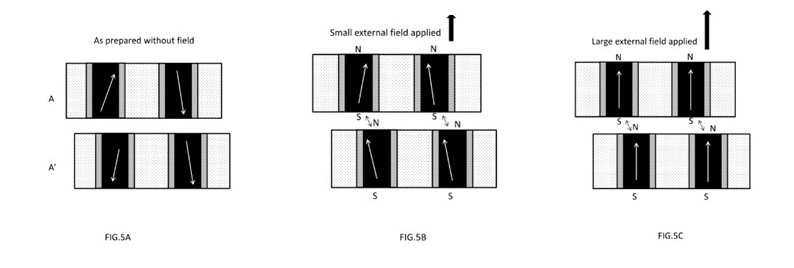
FIG. 5 (A-B) illustrates how the self-alignment principle works for the patterned magnet structured shown in FIG. 2A. FIG. 5A shows two components (wafer or chip) A and A′ with patterned magnet pairs for alignment when there is no external magnetic field exists. The magnetization representing by the white arrows has a random orientation pending on the aspect ratio induced magnetic shape anisotropy of the patterned magnets. In this illustration, the length of the patterned magnet is larger than that lateral dimensions. As such, the magnetization prefers to close to the longer length direction but has a wider distribution. FIG. 5B shows the magnetization alignment under a small magnetic field applied. All the magnetizations in the patterned magnets are aligned somehow but not at perfect alignment status (or not saturated). This causes the magnet southern (S) and Northern (N) pole also re-aligned. When the two components (wafer or chip) are approaching together after coarse alignment to ensures no mistakenly overlapping of the adjacent magnet pairs due to large lateral shifting roughly equal to distance between the adjacent magnet pairs during wafer bonding or chip-to-wafer bonding, the magnetic force between the S and N pole for the in-paired magnets will force to align together in order to minimize the overall the magnetic energy. When the external magnetic field increases, the decree of the alignment or saturation of the magnetization of the patterned magnets also increases, which is directly proportional to the magnetic force between the patterned magnets. When a large enough external magnetic field is applied, all the magnetization will be aligned as shown in FIG. 5C (patterned magnets are saturated). This will increase the magnetic force to the maximum between the magnet southern (S) and Northern (N) poles comparing to the case in FIG. 5B. If the magnets are made of the hard magnet materials such as CoPt, CoCr or CoCrPt etc, after alignment, even the external magnetic field is turned off, the alignment will still maintain due to its high coercivity Hc. For the soft magnetic materials case, after external magnetic field turn off, after the two components (wafer or chip) are joined, the aspect ratio will increases (e.g. doubled), the shape anisotropy will more or less maintain the magnetization orientation after bonding. Of course, the external magnetic field can be presented to enhance the force until the two components are fully bonded. For electrical via with built-in magnet shown in FIG. 3A, similar principle shown above will assist component (wafer or chip) alignment during binding.
About Effectual Services
Effectual Services is an award-winning Intellectual Property (IP) management advisory & consulting firm offering IP intelligence to Fortune 500 companies, law firms, research institutes and universities, and venture capital firms/PE firms, globally.
Through research & intelligence we help our clients in taking critical business decisions backed with credible data sources, which in turn helps them achieve their organisational goals, foster innovation and achieve milestones within timelines while optimising costs.
Solutions Driving Innovation & Intelligence


Enabling Fortune 500's, R&D Giants, Law firms, Universities, Research institutes & SME's Around The Globe Gather Intelligence That
Protects and Nurtures Innovation Through a Team of 250+ Techno Legal Professionals.