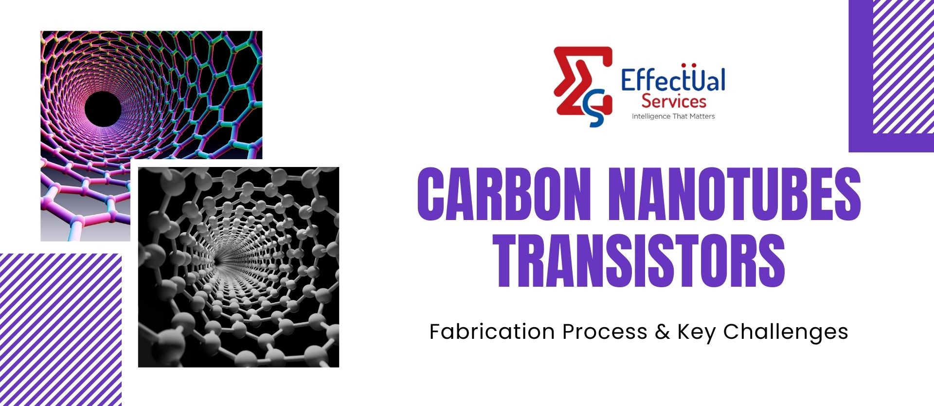
Carbon Nanotube Transistors - Fabrication & Key Challenges

Fabrication Process of Carbon Nanotube Field-Effect Transistors (CNTFETs)
The fabrication of Carbon Nanotube Field-Effect Transistors (CNTFETs) involves several critical steps to ensure precise CNT placement, alignment, and integration into electronic circuits. The process can be broadly divided into substrate preparation, CNT deposition, electrode fabrication, and device integration.
Step-by-Step Fabrication Process:
1. Substrate Preparation
- A suitable substrate is selected, typically silicon (Si) with a silicon dioxide (SiO₂) layer or a flexible polymer for flexible electronics.
- The substrate is cleaned to remove impurities using chemical treatments such as piranha solution or RCA cleaning.
2. Deposition of Gate Electrode and Dielectric Layer
- The gate electrode (bottom-gate configuration) is patterned using photolithography or electron-beam lithography (EBL).
- A thin layer of gate dielectric (e.g., SiO₂, HfO₂) is deposited using techniques like thermal oxidation, atomic layer deposition (ALD), or chemical vapor deposition (CVD).
3. Carbon Nanotube (CNT) Synthesis and Deposition
CNTs can be grown directly on the substrate or deposited from a solution:
- Direct Growth: CNTs are synthesized in situ using chemical vapor deposition (CVD), ensuring high alignment and purity.
- Solution-Based Deposition: Pre-synthesized CNTs are dispersed in a solution and deposited via methods like dielectrophoresis (DEP), spin-coating, or inkjet printing.
- CNT Sorting: Since CNTs exist in both metallic and semiconducting forms, separation techniques such as density gradient ultracentrifugation (DGU) or selective functionalization are used to ensure only semiconducting CNTs are used for transistors.
4. Source and Drain Electrode Fabrication
- Photolithography or EBL is used to pattern the source and drain contacts.
- Metals like gold (Au), palladium (Pd), or titanium (Ti) are deposited using electron-beam evaporation or sputtering, followed by a lift-off process to define the electrodes.
- The CNTs bridge the source and drain contacts, forming the transistor channel.
5. Annealing and Doping (Optional Step for Performance Enhancement)
- Annealing (thermal treatment) removes impurities and enhances CNT contact resistance.
- Chemical doping (e.g., with oxygen, nitric acid, or polymer functionalization) can be used to improve transistor characteristics.
6. Encapsulation and Final Processing
- A protective dielectric layer or polymer coating is applied for stability and reliability.
- Electrical connections and interconnects are added for circuit integration.
Read Also: Carbon Nanotube Transistors - Overview and Structure
Key Challenges in Carbon Nanotube Transistors (CNT-TFTs)
Despite their high potential as a silicon replacement, Carbon Nanotube Transistors (CNT-TFTs) face several technological and manufacturing challenges that hinder large-scale adoption.
1. Carbon Nanotube Purity and Sorting
CNTs exist in metallic and semiconducting forms, but only semiconducting CNTs are useful for transistors. Current synthesis methods produce a mix of metallic (~33%) and semiconducting CNTs, leading to uncontrolled transistor behavior. Advanced CNT sorting techniques like density gradient ultracentrifugation (DGU) and selective functionalization are being developed to improve purity.
2. CNT Alignment and Placement
Precise alignment of CNTs between source and drain electrodes is essential for high-performance transistors. Randomly distributed CNTs cause variability in electrical performance, reducing transistor efficiency. Techniques like chemical vapor deposition (CVD) growth on crystal surfaces, dielectrophoresis (DEP), and guided assembly are being explored for better alignment.
3. Contact Resistance at Metal-CNT Junctions
High contact resistance at the interface between CNTs and metal electrodes limits current flow. This leads to power loss, lower efficiency, and inconsistent transistor performance. Optimized metal-CNT contact engineering using palladium (Pd), titanium (Ti), or work-function-tuned metals, along with doping strategies, can reduce resistance.
4. Large-Scale Fabrication and Integration
Scaling CNT-TFTs for mass production while maintaining performance uniformity is difficult. Conventional lithography and deposition techniques are not optimized for CNT integration at an industrial scale. Printing techniques, roll-to-roll processing, and directed self-assembly methods are being explored for commercial feasibility.
5. Stability and Reliability
CNT transistors need to maintain long-term stability under real-world conditions. CNTs are sensitive to environmental factors like humidity, oxygen, and chemical contamination, leading to performance degradation over time. Encapsulation layers, surface passivation, and chemical treatments can improve device stability and longevity.
6. High Manufacturing Costs
CNT transistor production is still expensive compared to traditional silicon CMOS fabrication. High-purity CNT synthesis and sorting techniques add significant costs to the process. Innovations in scalable CVD growth, cost-effective separation techniques, and integration with existing semiconductor manufacturing processes are needed to make CNT transistors commercially viable.
About Effectual Services
Effectual Services is an award-winning Intellectual Property (IP) management advisory & consulting firm offering IP intelligence to Fortune 500 companies, law firms, research institutes and universities, and venture capital firms/PE firms, globally. Through research & intelligence we help our clients in taking critical business decisions backed with credible data sources, which in turn helps them achieve their organisational goals, foster innovation and achieve milestones within timelines while optimising costs.
We are one of the largest IP & business intelligence providers, globally serving clients for over a decade now. Our multidisciplinary teams of subject matter experts have deep knowledge of best practices across industries, are adept with benchmarking quality standards and use a combination of human and machine intellect to deliver quality projects. Having a global footprint in over 5 countries helps us to bridge boundaries and work seamlessly across multiple time zones, thus living to the core of our philosophy - Innovation is global, so are we !!!
Solutions Driving Innovation & Intelligence
Enabling Fortune 500's, R&D Giants, Law firms, Universities, Research institutes & SME's Around The Globe Gather Intelligence That
Protects and Nurtures Innovation Through a Team of 250+ Techno Legal Professionals.


