
Articles
The Future of Bioelectronics: How Flexible Electronics Are Transforming Brain Interfaces?
The Future of Bioelectronics: How Flexible Electronics Are Transforming Brain Interfaces?
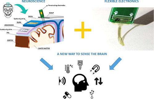
The brain is one of the most complex systems we can study, and neuroscience focuses on it. The enormous number of connections between cells and the various processes occurring at various scales result in a constant flow of data that must be gathered, evaluated, and interpreted. Neuroscientists attempt to dissect this complexity in order to uncover the fundamental ideas that underlie brain electrochemical signaling and human and animal behavior. By doing so, they can reveal the causes of neurodegenerative disorders and gain insight into the process of repairing damaged brain circuits. A neural interface, a technology that may connect with brain tissue at various levels to create a unidirectional or bidirectional communication line, is the primary tool for carrying out these tasks.
Recent innovations from a variety of fields have been merged to strengthen the capabilities and characteristics of neural interfaces. Among the several discoveries, flexible electronics is essential to the revolutionizing of brain interfaces.
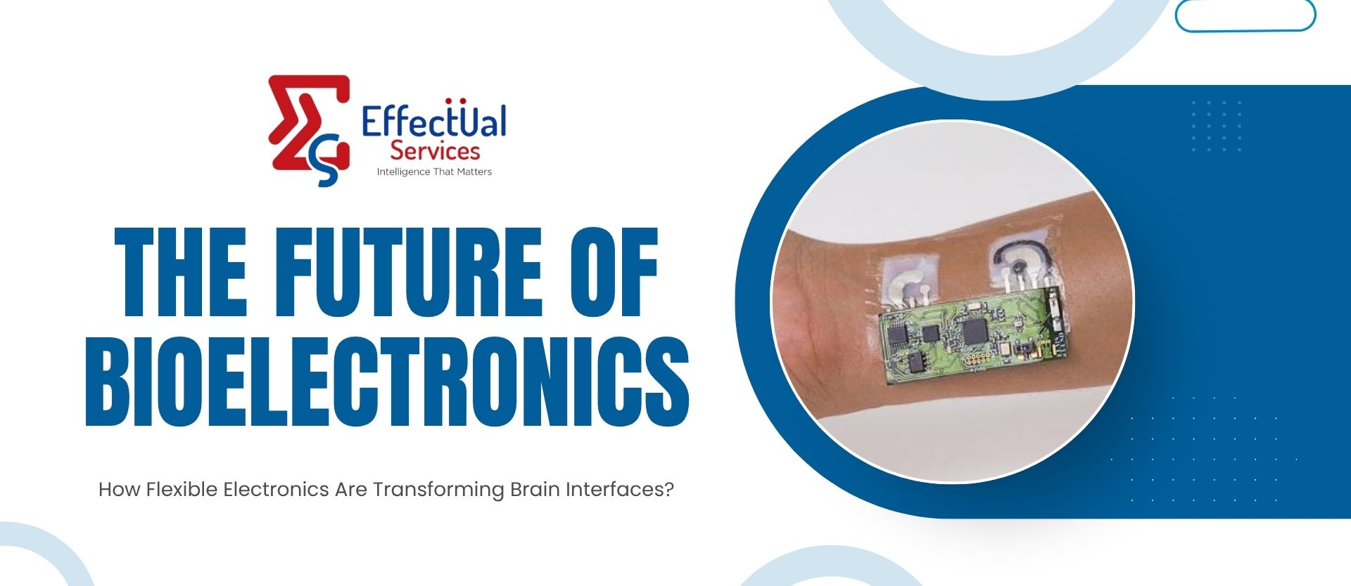
In order to control machines, brain-machine interfaces (BMIs) use sensors to gather electrical signals from the brain. While several prosthetic devices and treatments for epilepsy already use BMI-like systems, conventional probes can be uncomfortable and have subpar signal accuracy. But now, scientists have created adaptable BMIs that fit the brain. These could increase prosthetic control, advance the development of brain stents and brain monitoring technology, and better our understanding of brain disorders. Significant milestones have been reached since 2024, with companies such as Neuralink, Synchron, and Precision Neuroscience conducting active human clinical trials, demonstrating real-world feasibility of implantable BCIs. Future developments might someday enable full human-artificial intelligence interaction, but before that is widely adopted, ethical concerns must be taken into account.
The goal of the diverse field of study known as neuroscience is to explain how the central nervous system behaves. The ultimate goal of neuroscience is to establish a link between neural activity and behavioral patterns in living things. The difficulties are complicated, and a vast amount of morphological, functional, and physical data originating from the neural tissue must be gathered and examined. The findings are also challenging to achieve due to the enormous number of cells engaged in a single event and the variety of distinct events occurring from a single neuron to a big population of cells.
Studies on the behavior of dendritic spines and intracellular current, ion channel activation, and synaptic current at the scale of a single neuron are actually concentrated at the mesoscale, where smaller, more structured brain regions like cortical columns disclose certain activities. When brain areas interact on a wide scale, movement control, information processing, action inhibition, as well as emotion and idea generation, result. Everything we refer to as human behavior in actuality.
These three levels of information must be grasped and managed as they transit through the tiny, intricately organized regions of the neural system on their way from individual neurons to the functional parts of the brain. This entails coordinating inquiry analysis techniques that address the many problems and level of depth needed for a particular analysis. Large portions of the brain can be monitored using imaging techniques like functional magnetic resonance imaging (fMRI) and positron emission tomography (PET), or by mapping an external electrical activity with electroencephalography (EEG). The traditional approach, on the other hand, is a passive recording of neurons’ spontaneous activity or activity induced by some stimuli (that might be electrical, optical, pharmacological, etc.), which is used by electrophysiologists to collect direct information from specific areas of the brain.
The measurement of local field potentials (LFPs), which are produced by the superimposition of numerous potentials produced in the extracellular media by neuronal activity, is the foundation of this technology. The methods used to examine the behavior of a single neuron range from patch-clamp to two-photon imaging. All of these methods use various tools for gathering signals and understanding their nature, as well as varying degrees of intrusiveness.
Electronics now offers specialized tools for tracking the various brain functions and allows for the incorporation of fresh research methods. The traditional heavy laboratory apparatus, which is typically divided into distinct tools, has been replaced by new integrated devices that we refer to as brain interfaces. A neural interface, according to our definition, is a single electronic platform that can simultaneously record, amplify, digitalize, and classify brain signals. Depending on the needs, a neural interface may be entirely implantable or only partially implantable, although it is typically an intrusive tool. A neural interface can provide new electrophysiological options, particularly if it incorporates a stimulation sub-system. This is because it enables the use of closed-loop techniques that were previously restricted by the high latencies of older, more varied devices.
With the use of this platform, neuroscientists can gather data and identify distinctions between neurological illness patients and healthy individuals for both early disease identification and activity restoration. These neural interfaces can offer a rare chance for patients with tetraplegia or partial paralysis to partially regain some physiological functions or to establish neural bypass that would allow them to regulate hand gestures or limb motions.
Role of flexible electronics
Flexible electronics is becoming more and more significant in neuroscience with the goal of enhancing the functions of neural interfaces and controlling the quantity of information that may be detected during measurements. In order to fabricate bendable or rollable platforms on which electrical circuits and sensors are incorporated, flexible electronics requires a technology. Stretchable electronics are defined as circuitry that can be even slightly stretched without losing its functionality. When solar cell arrays were initially put together on a plastic substrate in the 1960s, this sort of electronics was born. The Brody group suggested the first flexible transistor during this time period, paving the way for active matrix liquid crystal displays (AMLCDs) to be developed in the 1990s.
The promise of printed organic electronics to significantly cut fabrication time and costs is seen in the 2000s. Chemists have created an enormous diversity of novel organic materials in recent years, opening up intriguing possibilities for a wide range of applications. In addition, different qualities can be added depending on the application, such as transparency (for smart displays used in automobiles), material biocompatibility (for biomedical devices), breathability (for skin smart patches), biodegradability (for low-cost disposable devices, for example in precise agriculture), and many others used in wearable applications, such as sportswear, smart toys, etc.
Using terminology from other electronic industries like consumer electronics, we can categorize active materials incorporated into flexible substrates into three main groups:
- Silicon-based materials
- Metal Oxide materials
- Organic materials
These technologies all display unique characteristics that make them each ideal for particular purposes. All of the aforementioned technologies are possible in biology, although inorganic-based electronics appear to be more durable. Biocompatibility, electrical and mechanical stability, electrical mobility, and process integrability are actually favored, especially in the case of long-term implants, despite the fact that biological events are inherently slow (usually not beyond kHz). When we take into account the rising demand for high-density recording systems with hundreds of channels that must be maintained in real-time, these considerations become more valid.
The use of a certain material also determines the technology utilized to produce the intended application: while roll-to-roll methods are favored for organic materials, conventional microelectronic equipment is employed for silicon and metal oxide devices.
Flexible electronics technologies
Local signal amplification is made possible by flexible electronics, which also offers potential closed-loop interaction and extra sensing features.
The integration of multiple electronic materials and components with different performances and production costs is proposed by several groups.
Here, we list the most cutting-edge fabrication techniques that have been included into BCI designs for both in vivo and in vitro uses. Each technology has unique benefits and inescapable disadvantages. Inorganic-based electronics, to put it briefly, perform better in terms of transistor electrical mobility, cut-off frequency, and material stability, but they require labor-intensive fabrication processes that are expensive to produce.
Organic electronics, on the other hand, can promise quick fabrication processes with more brain-like mechanical characteristics.
In any case, it must be noted that digitalization circuits and fast communication modules based on organic materials are still in their infancy and that hybrid solutions are chosen for the creation of the full brain interface.
Low temperature polysilicon technology
Low Temperature Polysilicon (LTPS) technology is an enticing option when compared to other active electronics technologies used in brain interfaces because LTPS has higher electrical stability and mobility than amorphous silicon, metal oxides, and organic materials. In addition, polysilicon provides the opportunity to produce CMOS technology and is completely compatible with high glass transition temperature polymers (Polyimide, Kapton, and Polyarylate) to create extremely flexible active grids. The performance of LTPS can be greatly improved even on extremely thin polymeric films with the aid of quick thermal treatments like excimer laser annealing (ELA), providing the ability to directly build electronics on plastic substrate without the use of a sacrificial layer.
ELA readily offers a polysilicon crystalline quality to obtain electrical mobility of roughly 50 cm²/Vs even if all manufacturing stages are restricted to a temperature of 300°C. These processes enable the production of tiny electrical components with channel lengths in the range of tens of microns without affecting the underlying polymer layer (often polyimide). The LTPS is a mature technology that is widely used in many commercial applications and prototypes. It is easily integrated with commercial chips built in crystalline silicon or other inorganic materials.
Large corporations throughout the world have embraced LTPS thin film transistors (TFTs) as a successful technology, particularly for the production of AMLCDs. To provide readout circuitry and the pre-amplification stage for flexible sensors and an ultra-flexible neural interface, LTPS TFTs-based circuits can be incorporated. Additionally, this technology offers strong chemical and mechanical stability, and it allows for the regulation of heat dissipation during operation by sandwiching particular layers (such as AlN, AlN/TiN, etc.) and appropriately adjusting TFT dimensions.
There have been many reports of tiny circuits and ultra-thin sensors based on LTPS. These parts serve as the basic building blocks for creating a dependable active grid to pre-amplify brain impulses, enabling improved performances with regard to organic electronics and attaining higher yield with regard to challenging crystalline silicon embedding technologies.
Crystalline silicon technology
A consolidated technology with tremendous electrical mobility (easily above 1000 cm³/Vs), amazing stability, and extreme downsizing is known as crystalline silicon-based electronics (CSE). Conversely, the manufacturing temperature, which is typically between 600°C and 900°C, prevents direct integration of CSE in flexible substrates. In any case, CSE is still a possibility for local amplification using deep electrodes. Despite these restrictions, researchers have described some methods for integrating CSE on flexible and stretchable substrates, including embedding silicon islands onto polymeric substrates or thinly encasing commercial chips in PDMS film.
Everything that is thin enough could become flexible. As a result, crystalline silicon can be bent to a thickness of just a few microns. We can see silicon membranes or islands integrated deeply into a plastic sheet where stresses trend to zero in accordance with the evaluation that the bending strains decrease linearly with thickness and taking into account that the bending strains are maximal at the surface of the device. These structures can withstand bends with radii that are a fraction of that of the material’s fracture limit. These techniques make it possible to produce functional circuitry near to the electrodes while taking advantage of the superior features of crystalline silicon technology. Additionally, CSE can be utilized to switch particular functionalities in the neural interface or to address and control huge electrode arrays.
The real yield of the devices, the inherent mechanical stress of the various layers of the chip stack (particularly for the wafer thinning technique), and the final substrate thickness, which in the case of ultra-thin chip packages is above 50 μm, are the limitations of this technology.
Due to the low etching effect between cerebrospinal fluid and silicon, biological fluid penetration into CSE is another crucial component to take into account. It poses serious safety risks. In any case, it is the principal cause of electronics degradation. In the conventional active electrode array layout, silicon dioxide barriers, especially for long-term implantation, can reduce these effects while also serving as the transistors’ gate dielectric.
Metal oxides
Another class of materials that is perfect for flexible electronics is metal oxides. Scientists have been examining the characteristics and capabilities of various alloys since the 2000s in an effort to develop a useful alternative to silicon technology for the consumer electronics sector. In 2003, Hosono demonstrated the first high mobility TFT based on Indium Gallium Zinc Oxide (IGZO) and provided a model for understanding the behavior of ZnO and related alloys. The success of zinc oxide-based alloys is then made possible by Hosono, Carcia, Martins, and Fortunato who explain the minor variations between amorphous and polycrystalline structures.
In 2007, Ju demonstrated the ability to deposit inorganic materials using a solution process approach, enabling the roll-to-roll manufacture of flexible electronics devices. This was a significant advancement for the metal oxide technology. Spray pyrolysis of metal oxides and solution methods using mixtures of metal oxides and 2D nanostructures are two more simple procedures.
Transparency in the visible range is these materials’ most alluring quality. Prins and Seager provided the first fully transparent TFT using SnO₂ and the first In₂O₃ non-volatile memory TFT, respectively, to illustrate this property for the first time. In theory, transparency in a particular light spectral band could make it possible to monitor brain activity while combining recordings with a visual method like two-photon calcium imaging.
Organic electronics
The main benefit of organic electronics and organic materials is that they are soft materials by nature. A lower Young’s modulus translates into improved mechanical compliance with living things and a greater capacity for stretching to accommodate devices with moving body parts. The combined electrical and ionic conductivity of these materials is also a distinctive quality. This characteristic makes low-impedance electrodes possible and is essential for sensing biological signals. Consumer electronics, which offer high contrast and high brightness flat panel displays based on organic light-emitting diode (OLED), have once again been the first to push organic electronics innovation. Then, organic materials have been widely used in organic thin-film transistors (OTFTs) and organic solar cells.
A prominent example of these prototypes is the electronic skin, which is made up of a number of soft temperature and pressure sensors, as well as electronic tattoos. OTFTs have expanded from single devices to create sophisticated sensor arrays and extremely flexible electronic platforms. In the past 20 years, a wide variety of various polymers have been studied and synthesized, giving good conductors, semiconductors, and dielectrics new capabilities including biodegradability, printability, and even self-healing properties. Chemists, in particular, discovered enticing solutions for semiconductors that improved material stability and operability: among the many polymers, we can name tiny conjugated molecules like pentacene and blends of its derivatives, rubrene, polythiophene, etc.
Hybrid electronic interfaces
Although flexible electronics offers a collection of potent methods to create a comprehensive brain interface, technological limitations continue to prevent its widespread adoption. On the other hand, hybrid solutions—where some system components, such the digitalization and communication modules, rely on generic commercial electronics or specialized chips—are piquing the interest of a number of parties. The use of a hybrid technique enables effective powering, real-time processing of enormous amounts of data, implementation of dependable communication protocols, and other benefits while simultaneously maintaining gentle contact between the brain and the grid. However, because the hybrid approach adds a challenging component to the neural interface, its dimensions must be kept to a minimum. This strategy often aims to optimize the device for a single use, occasionally creating ad-hoc integrated circuits with a set of specialized, constrained properties.
The hybrid system must be enclosed in an external case to be made bio-inert, which serves the dual purpose of shielding the electronics from biological fluids and disguising them from the body’s immune system. These factors emphasize the critical importance that an external case’s proper design plays in determining the effectiveness of a neural interface, particularly for long-term implants.
Interconnects for flexible electronics
Interconnections and linking techniques must be specifically discussed in every flexible system. In fact, because of the device’s intricacy, several foils are typically coupled to one another to create a neural interface. In order to achieve this goal, typical bonding procedures are inefficient on polymers or ultrathin metal layers, and maintaining adequate adhesion between several layers is not an easy task. These interconnections must endure elongation and distortion without losing their conducting qualities.
Nevertheless, more sophisticated methods like ink-jet or screen printing, flex-to-flex bonding, metal-based liquids deposition, conductive paste, etc. can be used to complete this difficult task.
This work is made more difficult in stretchable electronics. According to the requested elongation and the size of the component, in these devices, several designed geometries must be adopted. In order to achieve this, buckled films ensure better performance at the microscale, while beehive or horseshoe shapes can ensure a reliable conductance for elongation up to 20% and 100%, respectively.
Finally, conductive sponge and Nano-mesh represent the most promising geometries at the nanoscale.
Applications
Invasive BCI development is beginning to get the attention of private investors in addition to governments, who are making major investments through a variety of national and international initiatives. According to all projections, the next ten years will be favorable, with significant advancements in neurorehabilitation and innovative therapies for long-term neurological illnesses. Indeed, advancements in wireless communication and electronics downsizing permit studies on animals that are free to move.
Invasive BCI prototypes have now been tested in human patients, marking a major transition from concept to clinical reality. Neuralink successfully implanted its N1 brain-computer interface in its first human patient, Noland Arbaugh, in January 2024, under its PRIME (Precise Robotically Implanted Brain-Computer Interface) Study. By mid-2025, the company had enrolled nine patients across four countries — the United States, Canada, Great Britain, and the United Arab Emirates. Patients have demonstrated the ability to control computers and digital devices using thought alone, with reported usage of up to 10 hours per day. In November 2024, Neuralink also announced the CONVOY Study, aimed at extending its device capabilities to control assistive robotic arms. Synchron’s Stentrode BCI, implanted via a minimally invasive endovascular route through the jugular vein, reported positive 12-month safety and efficacy results from its U.S. COMMAND study in October 2024. Six patients with severe bilateral upper-limb paralysis showed consistent brain signal capture and conversion into digital motor outputs without any device-related serious adverse events, meeting the study’s primary endpoint. Additionally, hybrid systems for electrophysiological and optogenetic research continue to develop, enabling fresh insights into how the brain functions.
Neural interfaces can also offer special applications to gather data at various scales, from a single cell to complex interactions among cell populations, for in vitro studies. The external environment exerts a significant influence on a living cell’s functioning through a variety of chemical and physical stimuli. Glial cells and neurons are not an exception. In order to stimulate adhesion, proliferation, and differentiation, particularly for in vitro applications, neural interfaces can be employed. In this case, the use of particular functionalization techniques or just the provision of distinctive mechanical/electrical stimuli for interacting with the cells to detect neuron signaling makes neural interface nanotexturing vital. Using periodic or disordered nanostructures, the nano-pattern can be created both top-down and bottom-up.
In vivo-like neurons and glial cultures can be created by using 3D neural interfaces, according to recent findings, giving researchers the opportunity to study actual cell behavior in vitro. Another crucial aspect for understanding in vitro neuron activities is ultra-flexibility. Monitoring the activity of brain slices from various animals, such as ferrets, working on living tissue rather than 2D cell cultures, can yield significant information. The Sanchez-Vives group has made significant discoveries within this protocol regarding the nature of slow oscillations and their purposes.
Future perspective about brain neural interface
When we consider the neural interface’s potential, it makes sense to suggest that these systems will naturally advance in line with the current technological revolution. Scalability and miniaturization are driving implants and probes toward incredibly small architecture with amazing extra features: functionalities like signal multiplexing, signal digitalization, data processing, pattern recognition, and data classification can be embedded all at once dramatically reducing latency and allowing a true bidirectional interaction with our brain. Artificial intelligence and deep learning are now playing an increasingly central role in this evolution, with recent advances significantly improving the accuracy and robustness of neural signal decoding. Multimodal data fusion, hardware-software co-optimization, and closed-loop control strategies are emerging as critical pillars for enhancing real-time BCI performance. Even if the electrical activity of neurons is still the key information to be detected and analyzed, other information can be incorporated in the monitoring of brain activities because the brain is actually a pulsatile organ where blood continuously flows into capillaries and veins.
Specific brain regions respond electrically to pressure and heat gradients, and neurotransmitters move from one side of the neural network to the other. These phenomena all take place at various temporal and geographic scales and have a close relationship to neural activity. Every time we conduct an electrophysiological experiment, we merely fail to record all these data. In fact, up until now, only isolated efforts have been documented to detect the abnormal presence of a particular neurotransmitter or to record the thermal fingerprint of a functioning brain, notably for neurological illnesses. The variable opacity of the brain tissue and the skull to the various electromagnetic probes that can be used to connect the brain with external devices or with other people is one of the major challenges to overcome.
The neural dust, an ultrasonic communication system based on subdural transceivers and numerous microscopic motes directly implanted in the brain, is one of the intriguing alternatives recently put forward by a team from UC Berkeley. Distribution of various technologies through the layer of the head is probably a workable strategy. For example, we might consider tattooing electronics to create communication modules and antennae on the skin, as well as inserting infrared or magnetic sources inside the skull to stimulate neurons. In any event, invasiveness is still up for debate.
Additionally, in the case of optogenetics, the potential for creating electro-optical circuits has not been fully investigated. Flexible electronics can offer distinctive ways to create a collection of creative circuits and sensors that could one day lead to a breakthrough in our knowledge of the fundamentals of neurological principles or in how to connect with our brain in fresh ways.
By using magnetic stimulation rather than electrical stimulation, which reduces concerns associated with materials loss during stimulation, the installation of micro-coils into the flexible grid should lessen the problem with tissue response for long-term implants. Additionally, extremely adaptable microfluidics might aid in developing a drug delivery system to offer patients with persistent neurological illnesses individualized therapy. Integration of optical and infrared source arrays could ensure direct activation of neurons in optogenetic research or the monitoring of blood flow. A landmark 2026 study published in Nature Machine Intelligence demonstrated a thin, flexible microelectrode array that can be introduced through a small slit in the skull onto the brain surface, achieving high-resolution brain–computer interfacing in both animal and early human pilot studies — pointing toward a new generation of minimally invasive yet high-fidelity neural interfaces. Finally, a successful bidirectional contact could enable future scenarios that enable brain-to-brain connectivity or brain-to-machine interoperability or allow patients with paralysis or injury to the peripheral nervous system to naturally control certain body parts.
Future neural interfaces might incorporate the following technologies: infrared-based communication module, reliable bidirectional communication, local temperature and pH sensors, magnetic stimulation, embedded drug delivery capabilities, and even brain-to-brain connectivity. The integration of AI-driven signal processing and closed-loop feedback systems is expected to accelerate the path from experimental prototypes to clinically approved devices. To make it possible, flexible electronics is a prospective ally.
Please feel free to reach out to one of our subject matter experts at info@effectualservices.com to explore, how we can help you & make the world a better place to live in !!!
About Effectual Services
Effectual’s BIOELECTRONICS & NEUROSCIENCE TECHNOLOGY RESEARCH FRAMEWORK is a deep dive into this ecosystem and shall help you understand the intricacies of this nascent innovative domain with insights backed with credible data sources. Some ways we can help include, but not limited to — Performing any previous art or freedom to operate searches to help you better grasp the environment surrounding your invention or business endeavors. If certain methods of IP protection are more appropriate for your technological or business goals, we can help you strategize effectively to plan for future & in making continuous innovation a part of your working model.
Solutions Driving Innovation & Intelligence


Enabling Fortune 500's, R&D Giants, Law firms, Universities, Research institutes & SME's Around The Globe Gather Intelligence That
Protects and Nurtures Innovation Through a Team of 250+ Techno Legal Professionals.